580 California St., Suite 400
San Francisco, CA, 94104
This research area focuses on advancing hardware implementations for BCD arithmetic operations, especially addition, subtraction, and multiplication, to meet the demands of decimal-intensive applications such as financial computations and embedded systems. It is motivated by the need for faster, more area- and power-efficient decimal arithmetic units that preserve decimal precision and integrate well with existing digital systems.
This theme explores methodologies for encoding decimals into binary formats that preserve numeric order while supporting arbitrary precision and range. Such encodings are crucial for database indexing, compression, and retrieval where fast lexical sorting of encoded decimals corresponds to their numeric order, allowing efficient similarity search, storage, and streaming data applications.
This research area investigates the use of reversible logic gates—such as Toffoli and Fredkin gates—for the implementation of energy-efficient and low-heat-dissipation BCD adders and arithmetic units, pertinent to nanotechnology and quantum computing. It also examines optical computing designs and novel hardware realizations aimed at improving speed and reducing power consumption in decimal arithmetic.
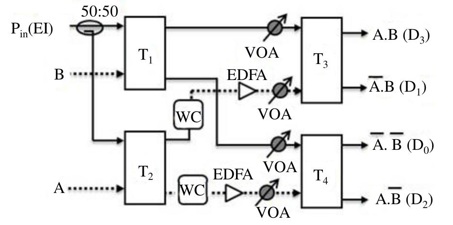
![Figure 1. A TOAD based optical switch with single control pulse (CP), where SOA: semiconductor optical amplifier, CW: clockwise pulse, CCW: counterclockwise pulse, t,: pulse round trip time, Ax: asymmetric distance, IS: incoming signal and OC: optical circulator. with a being the line-width enhancement factor. In the absence of a control signal, data signal (incoming signal) enters the fiber loop, pass through the SOA at different times as they counter-propagate around the loop and ex- perience the same unsaturated small amplifier gain G,, and recombine at the input coupler i.e. G,.., ~ G.,. Then, Ag = 0 and expression for P,, ~ 0 and Prow (t) =P (t)-G,, . It shows that data is reflected back toward the source. When a control pulse is injected into the loop (CP = on), it saturates the SOA at time f, and changes its index of refraction. The gain of the SOA decreases rapidly as [11 ]-[13]:](https://figures.academia-assets.com/108023720/figure_001.jpg)
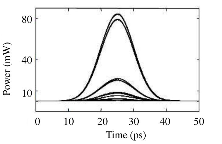
![Figure 5. Variation of CR with (a) control pulse energy and gain recovery time and (b) gain recovery time and puls« width at the outputs. This in turn means that less energy is required in order to saturate the SOA and obtain a large change in the amplification of the counter-propagating pulses. The value of ~100 fJ for control pulse energy, ~100 ps for gain recovery time and pulse width ~ 2 ps is applied for getting the contrast ratio greater than 9 dB. The lower con- trol pulse energy and small-signal gain values are insufficient for full switching. This occurs because the created phase difference is much less tha superposition of the outputs for t n the required value 2, which reduces the contrast ratio. The eye-diagram is the he repetition period of the inputs, i.e., inputs varies from 0-0, 0 1, 1> 1, 1> 0, and so on [14]. Figure 6 is called a pseudo-eye-diagram |14|. The relative eye opening (O) is defined as min max Fase d P° are the minimum and maximum powers at 1-state and 0-state, respec- max O=(Plin—Phax)/Phin > Phin aM ost which can be calculated from Figure 6. An eye-diagram with large eyes indicates a clear transmission with a low bit error rate. Here, we get PED (O) = 82.36%, which indicates an excellent response of the circuit to the incoming data at its output terminals.](https://figures.academia-assets.com/108023720/figure_004.jpg)
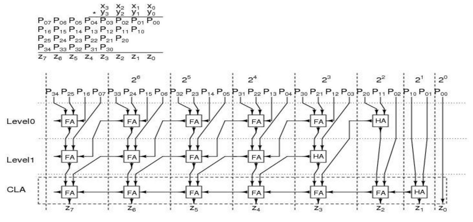
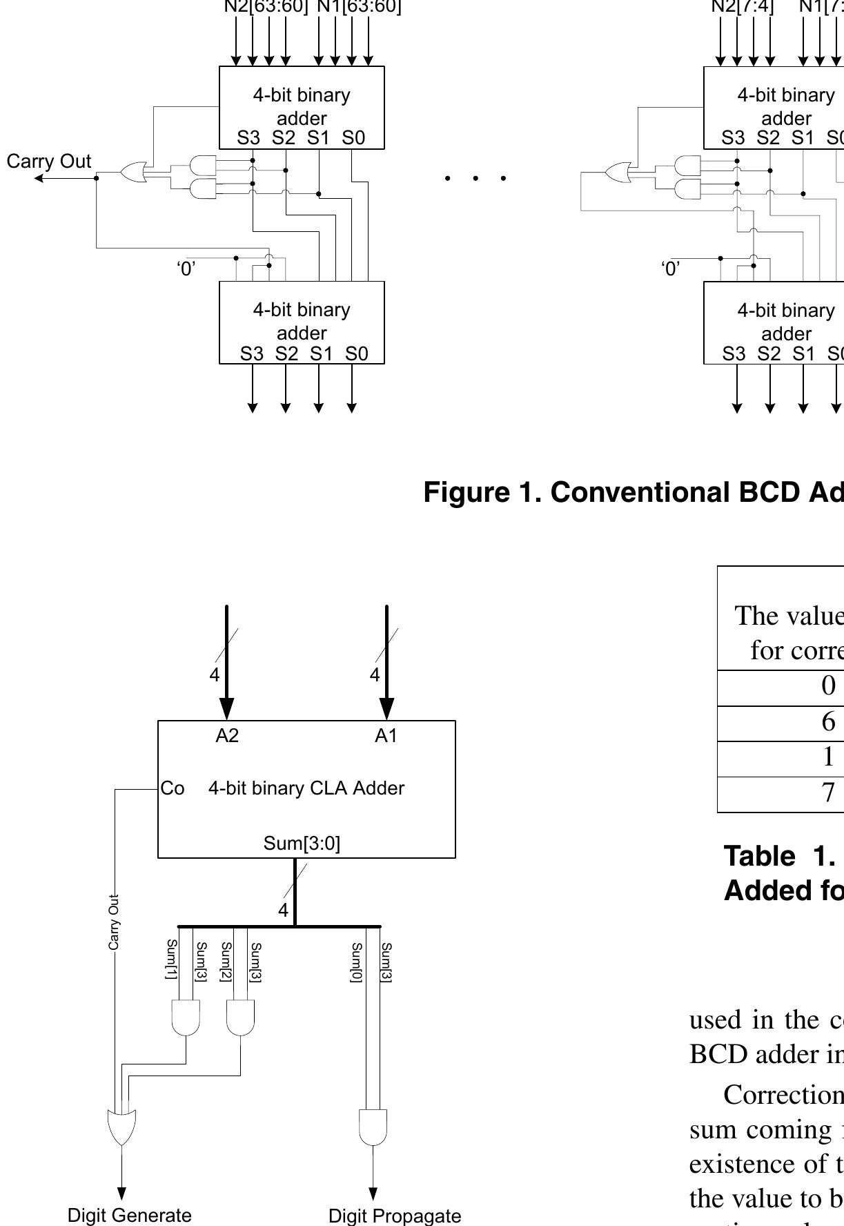
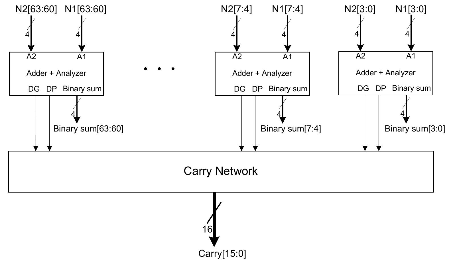
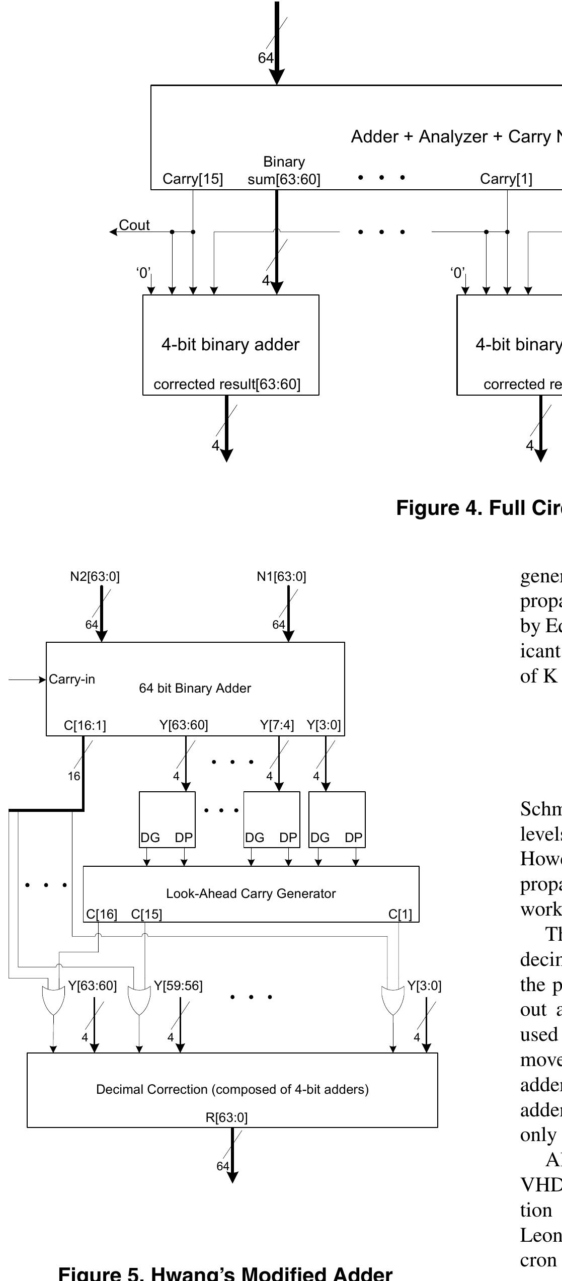
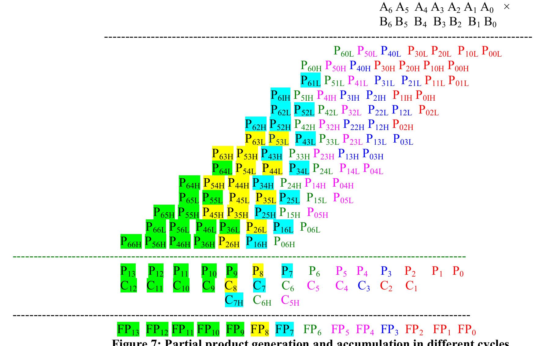
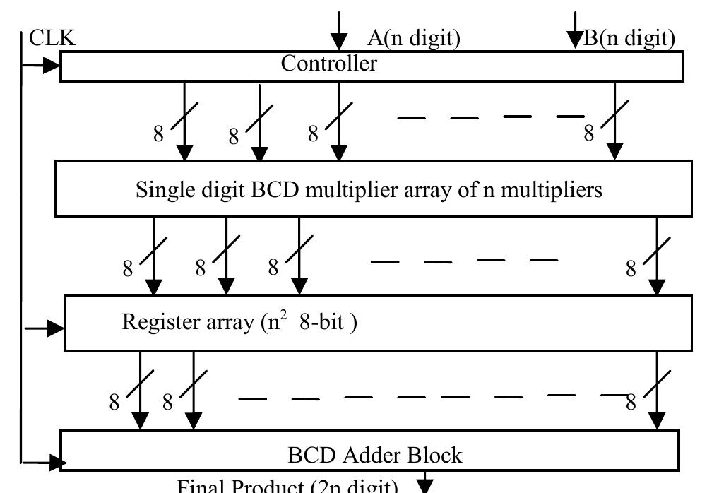
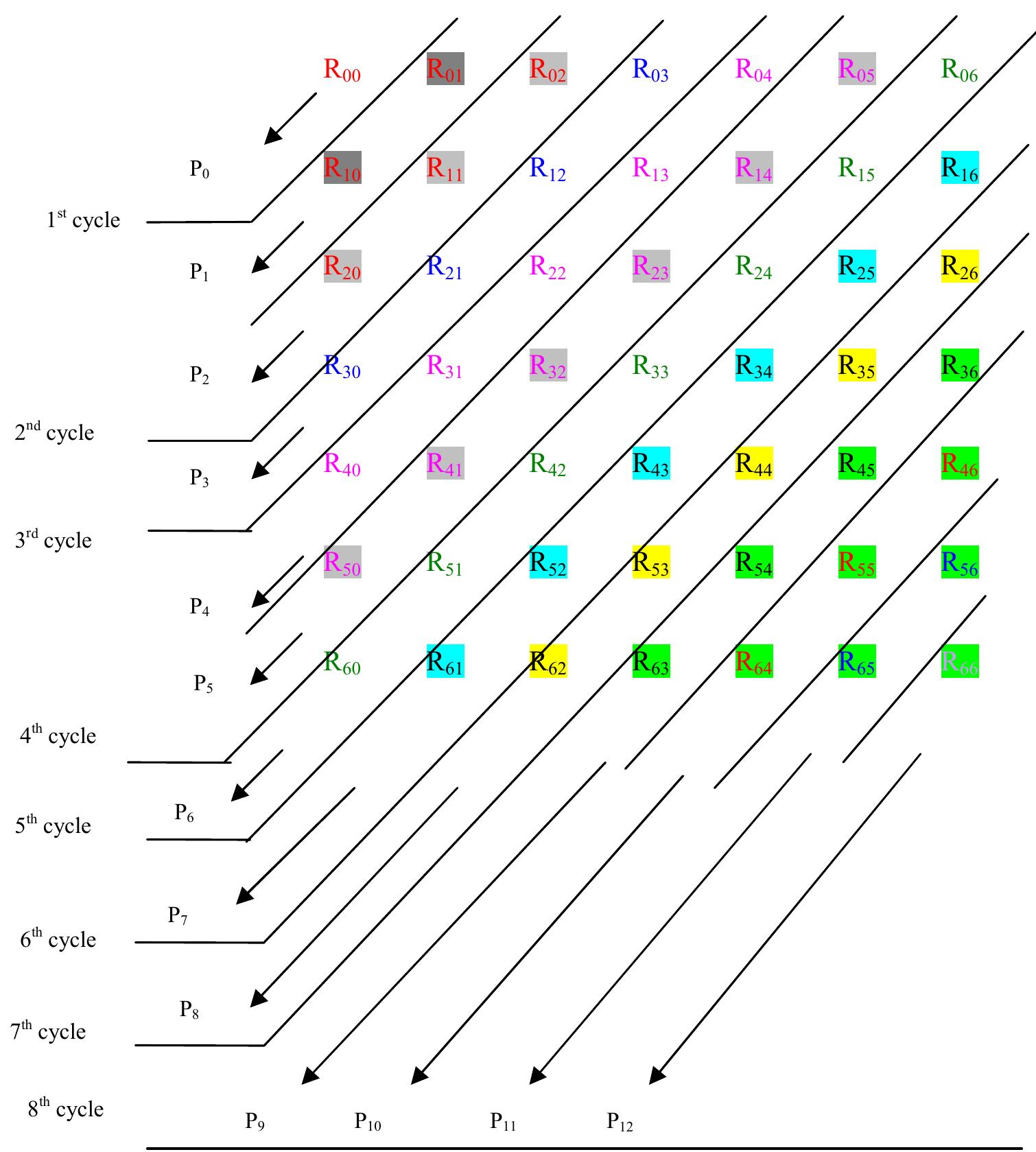
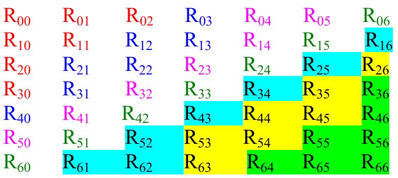
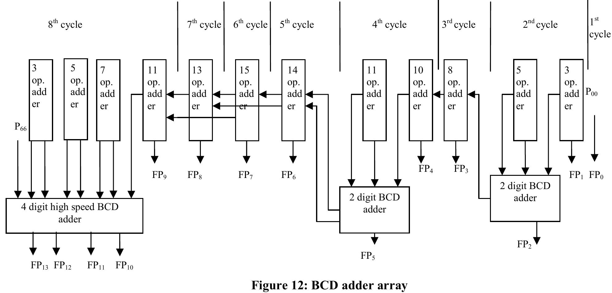
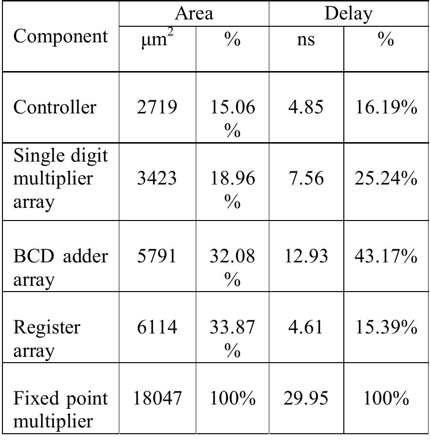
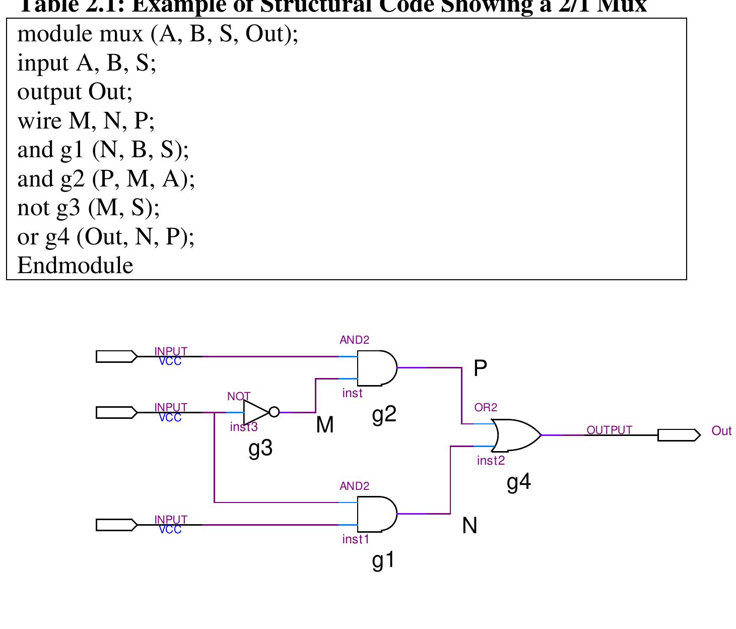
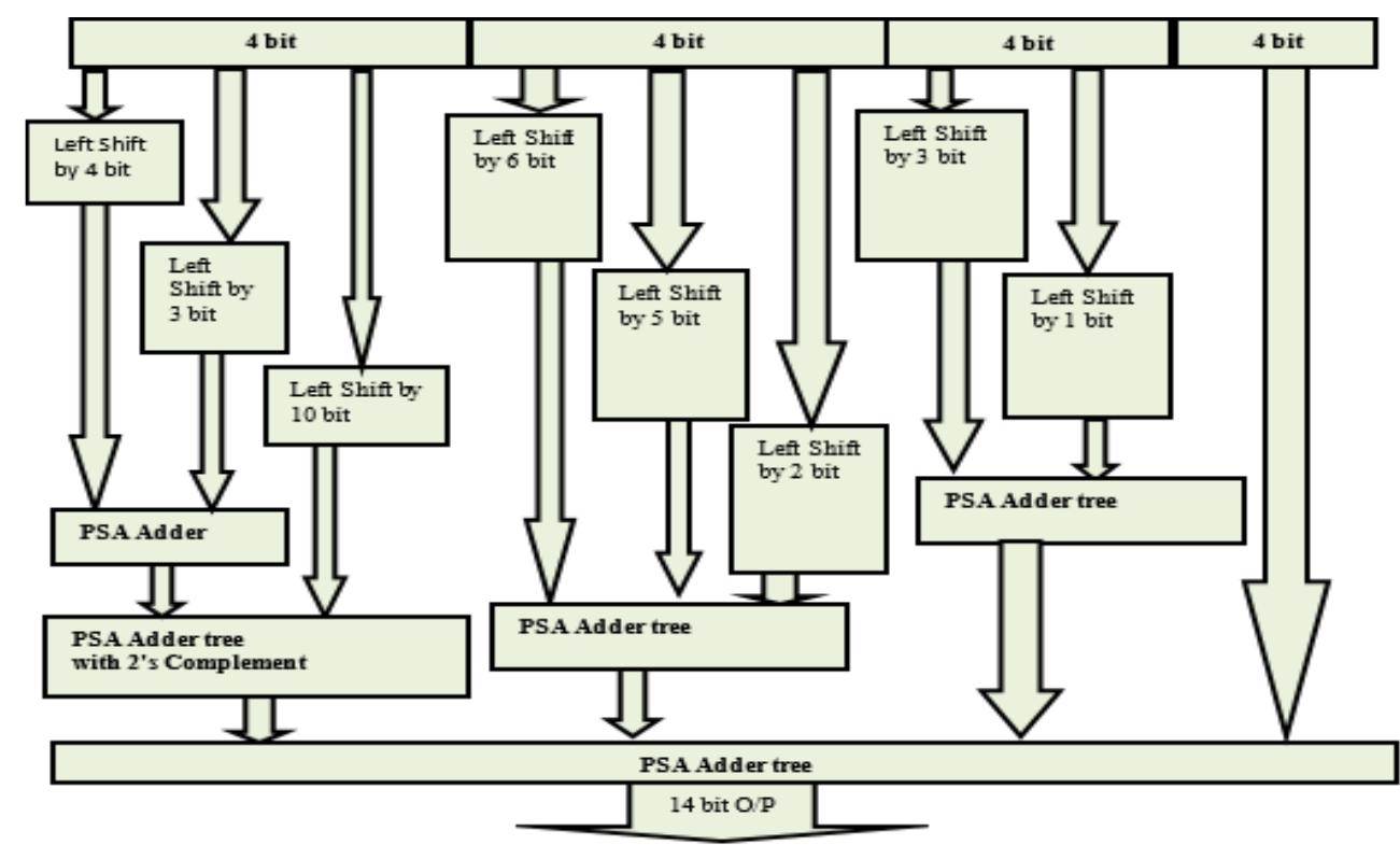
![Table 1: Comparison of area and delay of single digit BCD multiplier implementations 3. Decimal Fixed Point Multiplication The fixed point multiplier unit takes two n-digit operands, calculates n’ partial products and returns their sum as a 2n-digit integer. There are two main stages in the fixed-point multiplier design: generation of partial products and reduction of partial products. In the first stage of the process, the RPS algorithm selects appropriate inputs for generation of partial products using n single digit multipliers. After the generation of partial products they are reduced along with the carry of previous addition using multi-operand decimal adders. The process is repeated n times to generate a 2n digit product after the (n+1) ™ cycle. Many techniques have been developed to speed up the process of decimal addition. Direct decimal addition is one of the efficient techniques for two-operand decimal addition [11]. Erle and Schulte proposed a variant of direct decimal addition to produce intermediate results in a decimal carry-save format that can be used in an iterative decimal multiplier [12]. In another approach, proposed by Ohtsuki et al., a correction value of six is added to each digit of the first partial product using a binary carry-save adder [13]. Shirazi et al. proposed a technique for constant time decimal addition, called Redundant Binary Coded Decimal (RBCD) [14, 15]. Kenney and Schulte introduced three algorithms for performing fast decimal addition on multiple BCD operands: non-speculative tree, double correction speculation array and single correction speculation array [16]. The non-speculative tree algorithm that gives the minimum delay with same area of the three algorithms is the best suited for multi-operand decimal addition and is made use of in this research. In [17] a new scheme is proposed to obtain the sum of each decimal column via a network of carry-free adders and converting the sum into decimal format via a fast binary to decimal converter.](https://figures.academia-assets.com/105583075/figure_004.jpg)
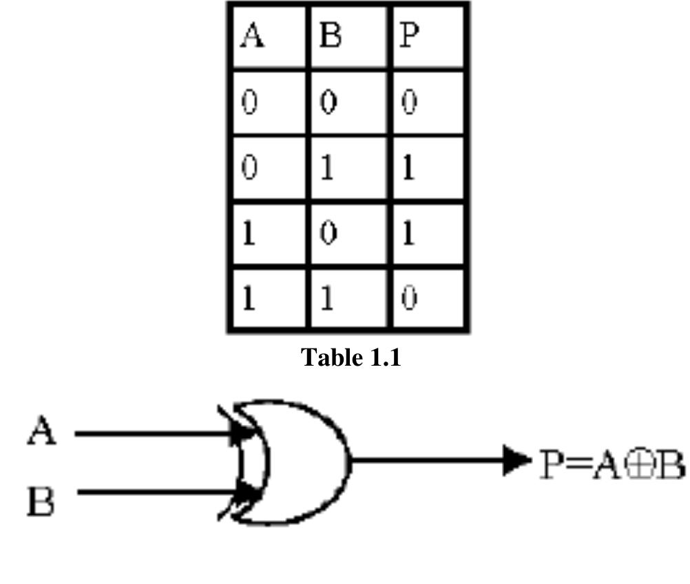
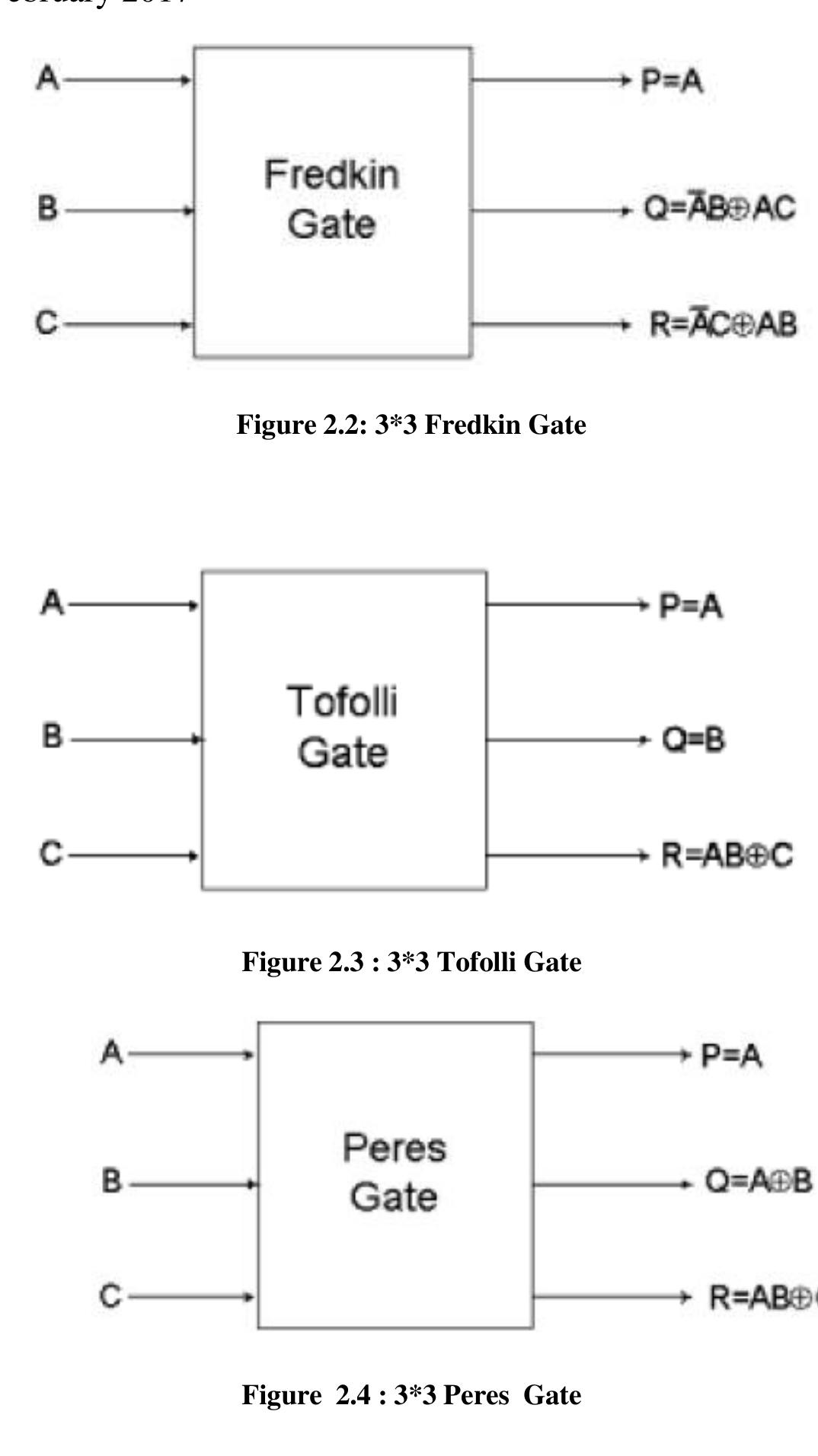
![II. Reversible Logic Gates There exist many reversible gates in the literature. Among them 2*2 Feynman gate [6] (shown in figure2), 3*3 Fredkin gate [7] (shown in figure 3), 3*3 Toffoli gate [8] (shown in figure 4) and 3*3 Peres gate [9] (shown in figure 5) is the most referred. The detailed cost of a reversible gate depends on any particular realization of quantum logic. Generally, the cost is calculated as a total sum of 2*2 quantum primitives used. The cost of Toffoli gate is exactly the same as the cost of Fredkin gate and is 5. The only cheapest quantum realization of a complete (universal) 3*3 reversible gate is Peres gate and its cost is 4. nternational Conference on Mechanical, Energy & Power Systems](https://figures.academia-assets.com/103562756/figure_002.jpg)
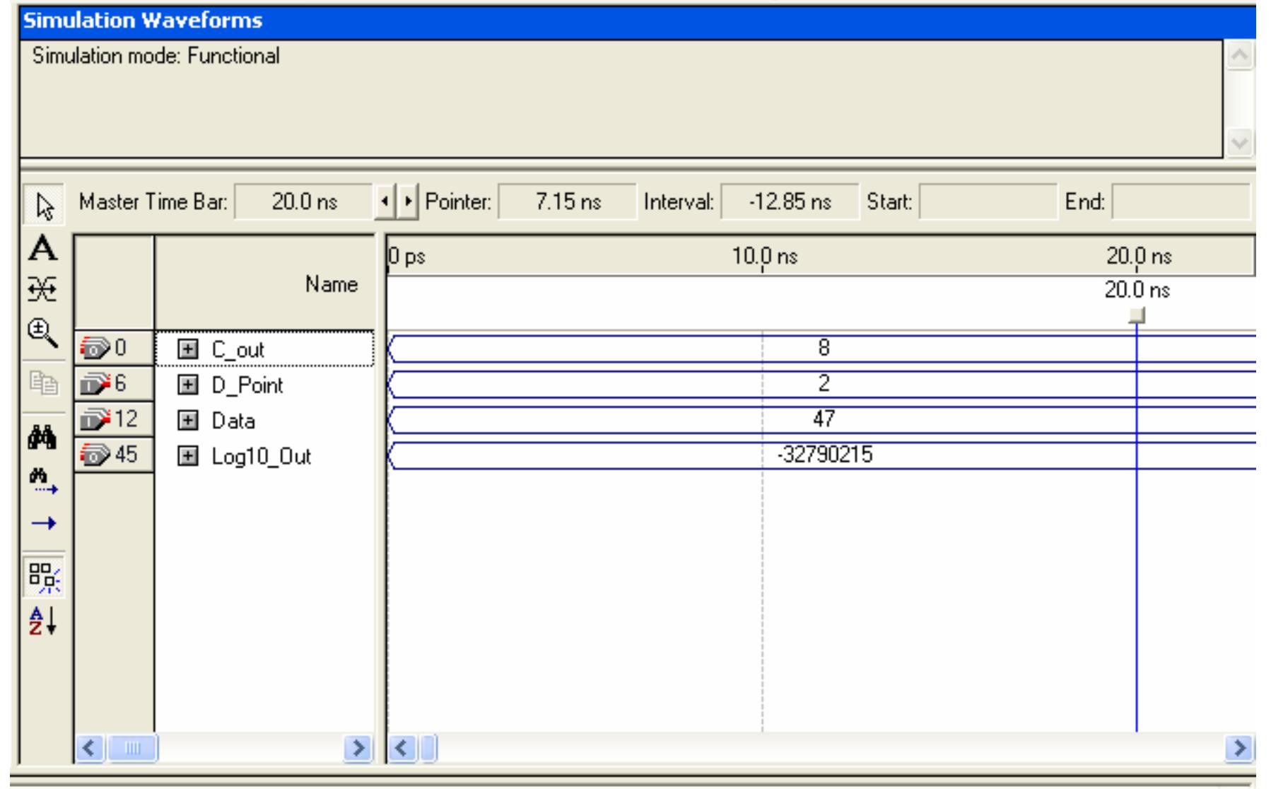
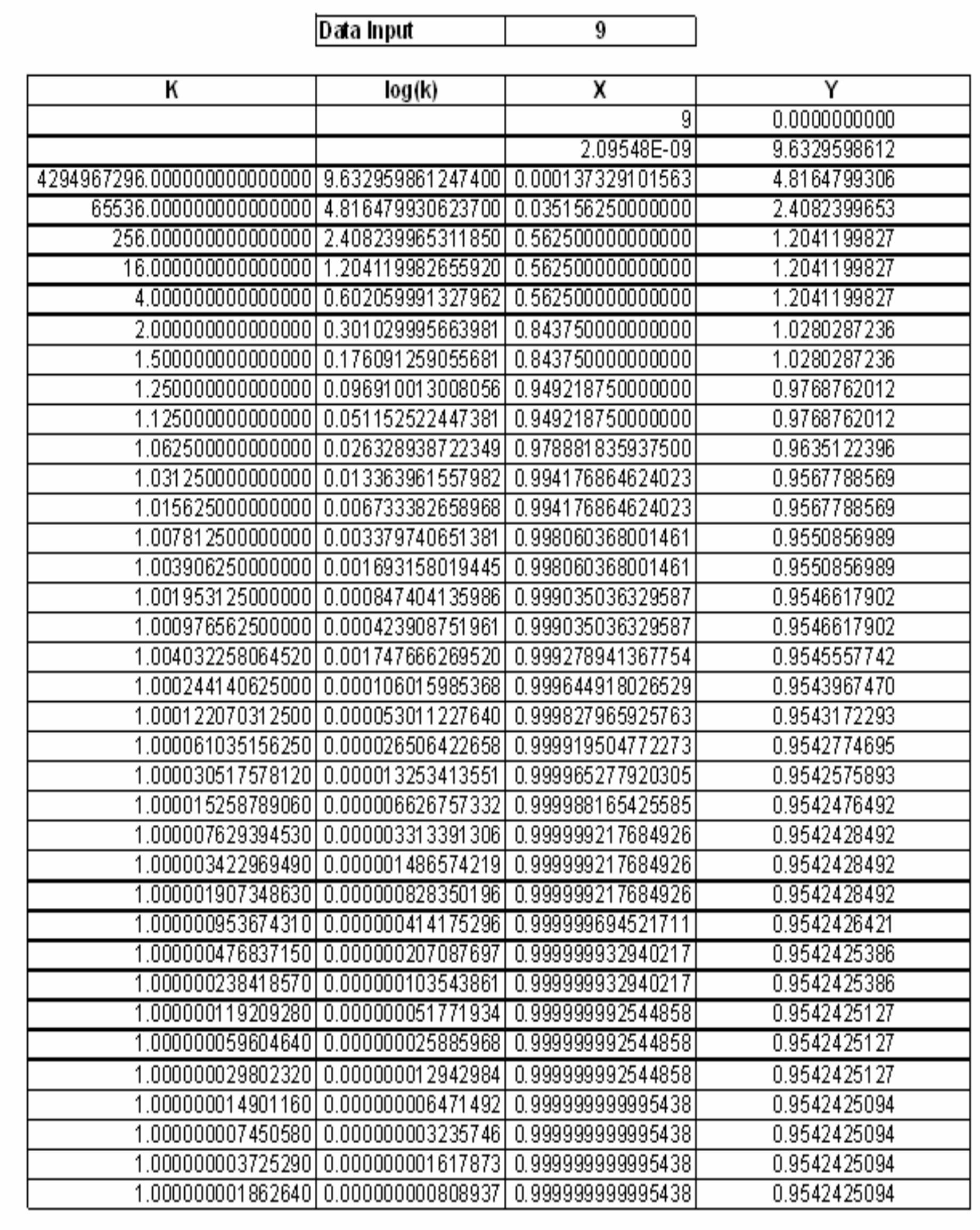
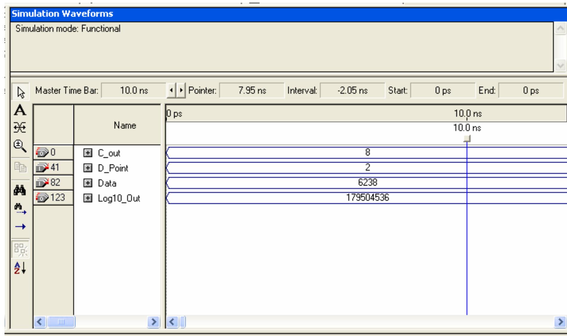
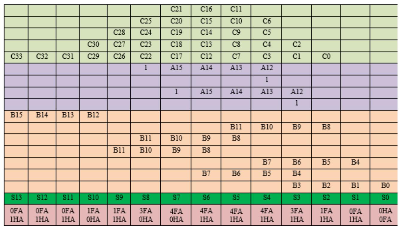
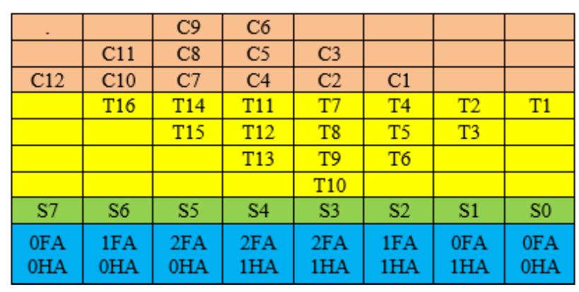
![Figure 7. BCD multiplication simulation observed on Xilinx VIVADO-ISE The register transfer logic entries are done using very high-speed integrated circuit hardware description language (VHDL) in the proposed design. Synthesis is done for combinational style modeling and the target device selected is Zynq-7000 FPGA. Figure 7 shows the simulation result obtain for this 16x16 radix-10 multiplier design; this result generated using the integrated simulation environment (ISE) of Xilinx Vivado [14]. A few other simulation observations are shown in Table 2. Row-1 of Table 2 shows the observation of the ISE simulator shown in Figure 7.](https://figures.academia-assets.com/93932036/figure_007.jpg)
![Table 3 shows the Synthesis results for the proposed 16x16 BCD multiplier design, observed using the Xilinx Vivado tool [14] and Zynq-7000 Field programmable gate array (FPGA) [14]. From Table 3 it may observe that numbers of Zynq-7000 FPGA slices used in this work are 482 and also the Maximum frequency obtain is 267.251 Mhz. The simulations are observed for a balanced Simulator setting in Xilinx VIvado. The area obtains for the proposed work design implementation is 0.04138 mm*. The number of universal gates two input NAND required for this design is 29362.](https://figures.academia-assets.com/93932036/table_002.jpg)
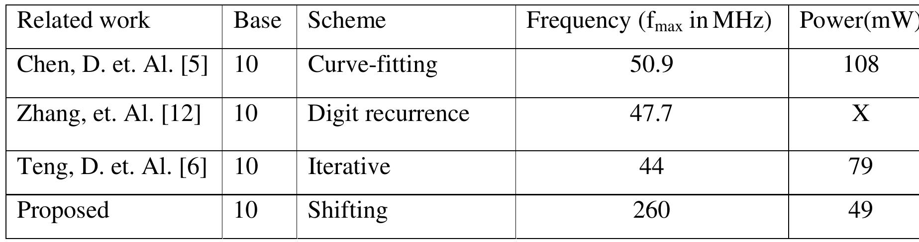
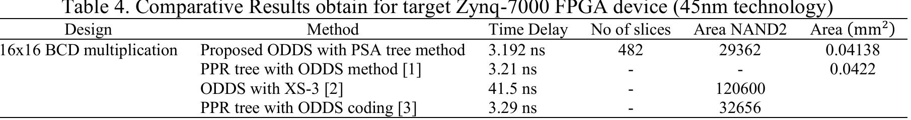
![Table 4. Comparative Results obtain for target Zynq-7000 FPGA device (45nm technology) Table 4 shows the different methods used and by researchers and proposed method with the time delay results. The results are obtained using the HDL based FPGA implementation. This work is an application specific integrated circuit (ASIC) design and the target device FPGA technology must be the same for comparison, hence this work has selected FPGA of 45 nm technology same as of [1-3]. It is observed that the time delay for the proposed design of 16x16 BCD multiplication is lowest among other related works for the same platform. from the table, it may also observe that the area requirement of proposed work is less as compared with other work.](https://figures.academia-assets.com/93932036/table_003.jpg)
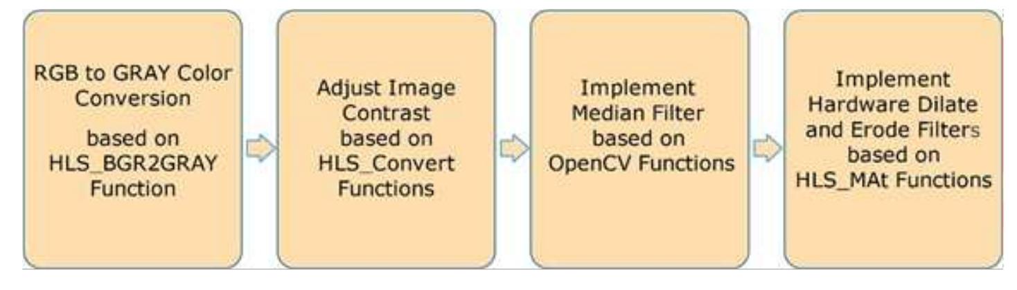
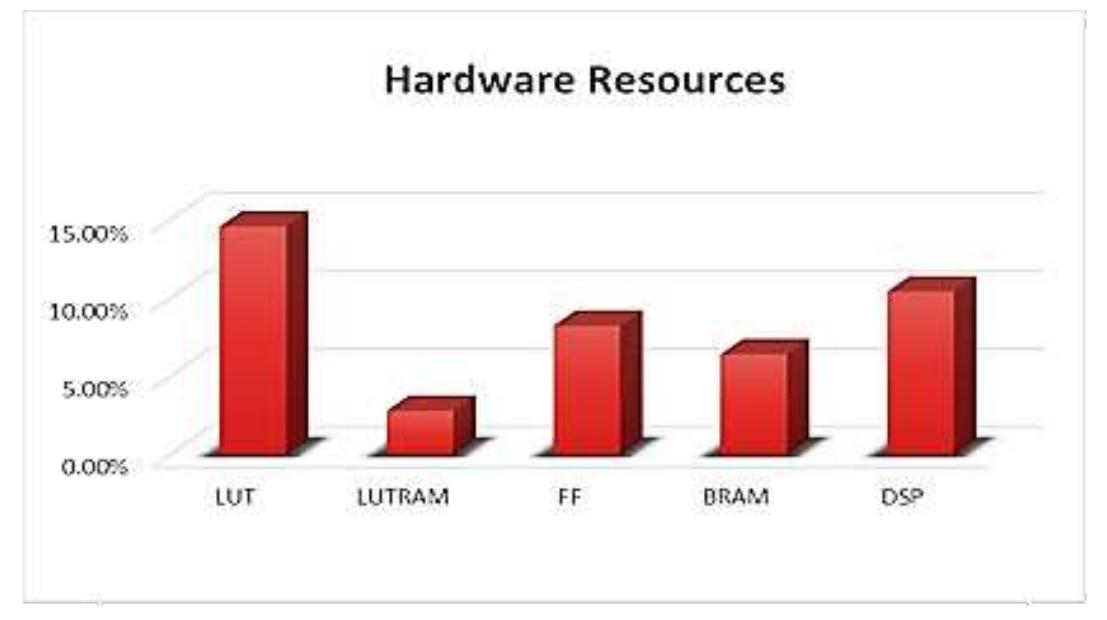
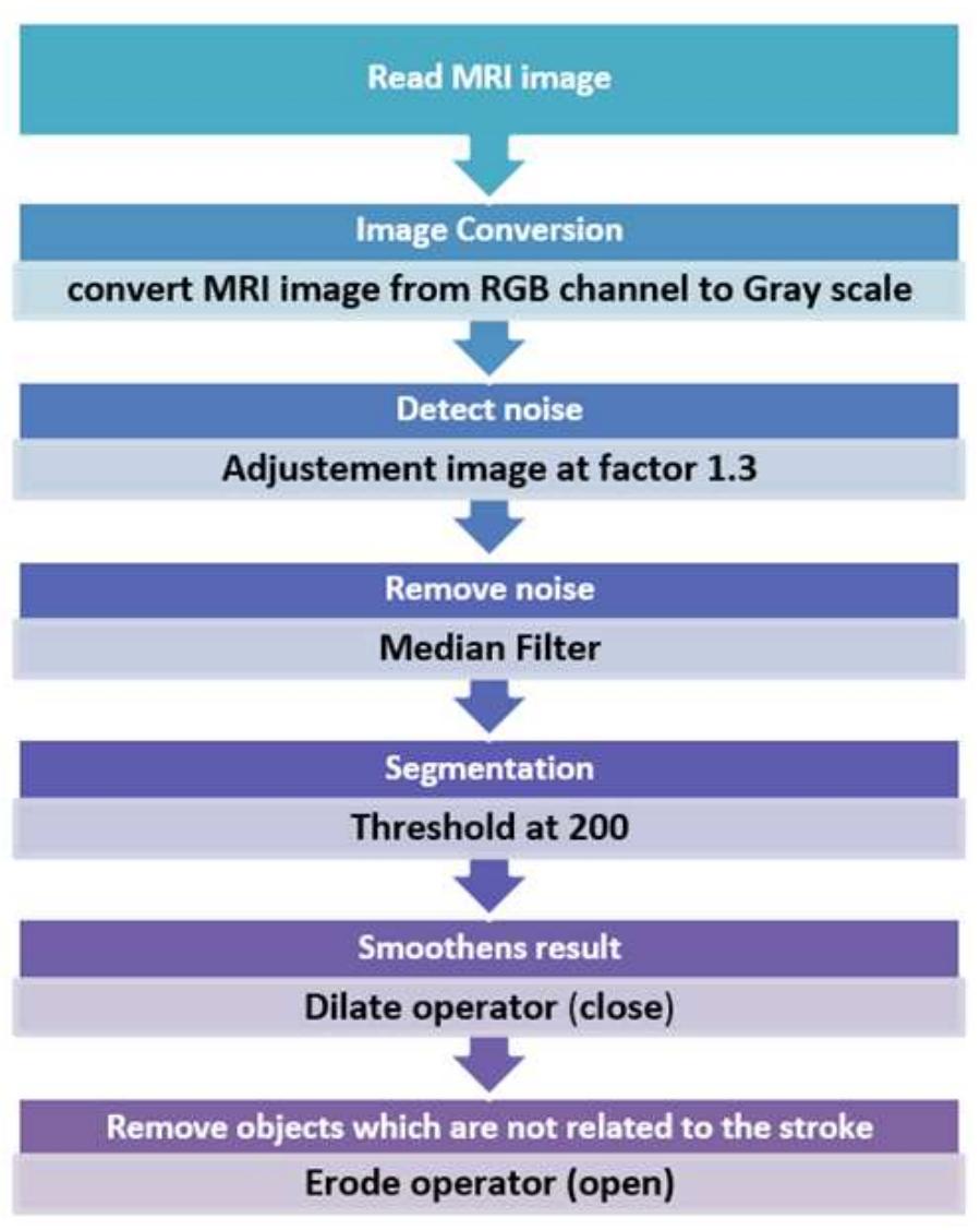
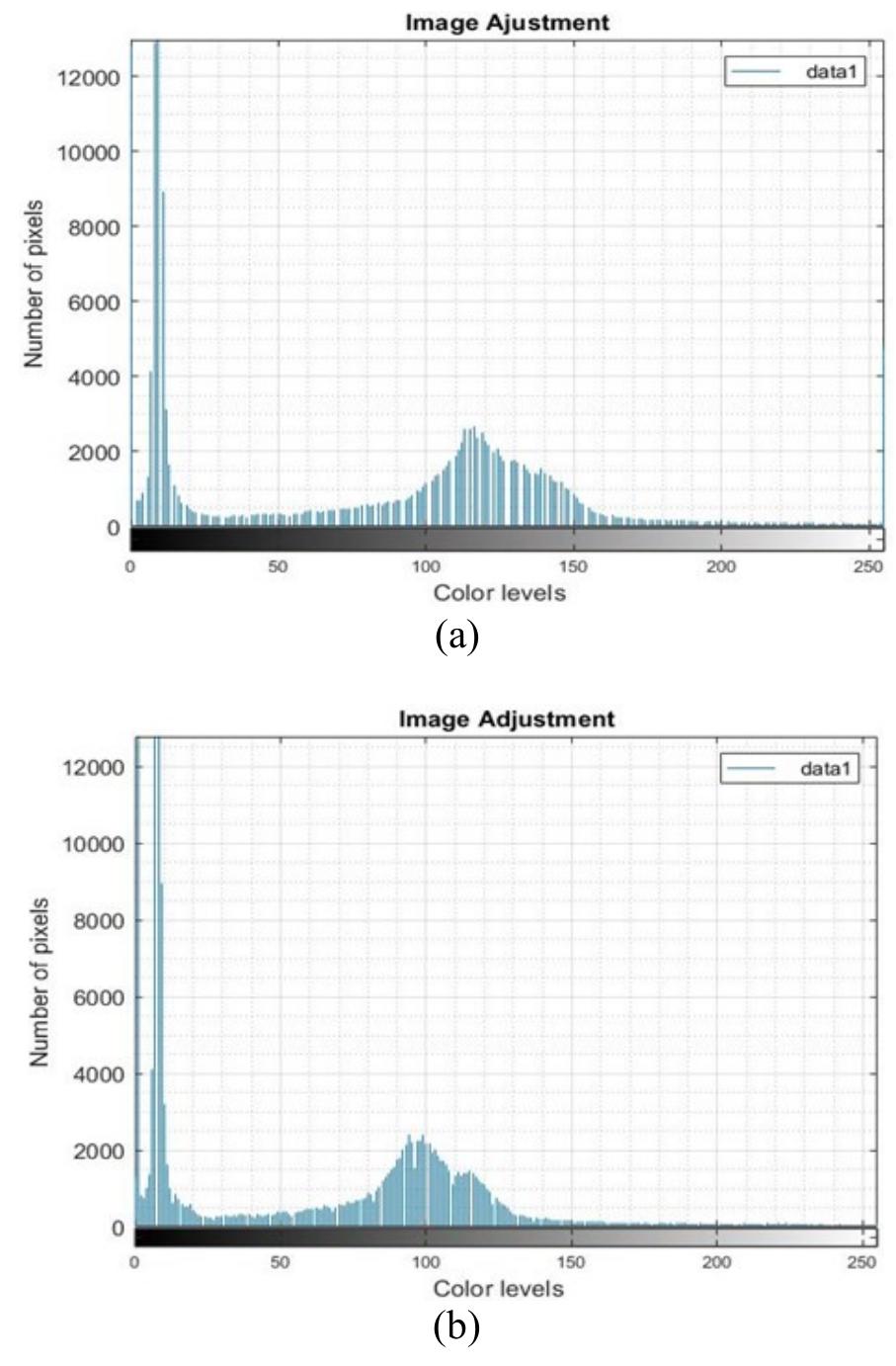
![Figure 2. Overall proposed system on zynq chip The Zynq AXI lite interface connection is used to implement the proposed system as illustrate in Figure 2. 5. RESULTS AND ANALYSIS The hardware resources for entire system are summarized in Figure 3. The Zynq xc7z020 evaluation kit comprise [30] 53200-LUT (lookup table), 106400-FF (flip-flop), 140-BRAM (block RAM), 32-BUFG, and 220-DSP (digital signal processor) block. While the implementation needs: 15% (7773) of LUT, 3% (491) of LUTRAM (RAM lookup table), 8% (8793) of FF, 6% (9) of BRAM, and 10% (23) of DSP block. In order to test the effectiveness of the proposed system, two different MRI images of brain strock are applied to our FPGA design. Then, the results are compared with Matlab program to measure the efficiency of our system as illustrated in the following flowchart: Acpocnardingo tra the Biogire 4 the flauschart inclidec the fallauzing ctenc:](https://figures.academia-assets.com/83175617/figure_002.jpg)